On-chip bus
The virtual on-chip bus that is used by the IPbus transactor (as master) and by the IPbus firmware slaves is based on the Wishbone SoC bus. It is typically used in hierarchical topologies, with signals multiplexed to several slaves at each layer. There are a couple of notable difference from Wishbone in the signalling protocol, as outlined below.
Bus topology
The bus is implemented as a set of point-to-point signals. Connection of multiple slaves therefore requires an address decoder and logic to multiplex read data from the slaves back to the master connection, referred to as “bus fabric” in the diagram below; the ipbus_fabric_sel entity from the repository (components/ipbus_core/firmare/hdl/ipbus_fabric_sel.vhd) implements this multiplexing functionality.
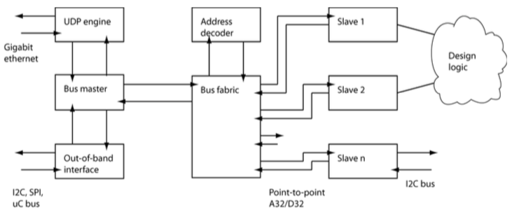
The bus fabric arranges for a slave to see activity on the bus when it is being addressed. It is therefore necessary for a slave to decode only its internal address space, and it need have no knowledge of the its position in the overall A32 address space.
Designs need not use either the full A32 or D32 width, and the unused logic should be optimized away in this case.
Clocking
The on-chip bus is fully synchronous, and operates from a single system clock. There is no constraint on the relationship of the bus clock to the transport interface clock (e.g. the 125MHz GbE clock or the PCIe clock), as the firmware for each transport interface contains handshaking logic.
For slaves which do not require wait states, the 32b data path on the bus allows full utilization of a Gigabit Ethernet interface as long as it runs at >32MHz; this allows straightforward timing closure for complex multi-slave designs. Ethernet-based designs therefore typically drive the IPbus clock at 1⁄4 of the GbE clock (i.e. 31.25MHz).
Bus signals
The bus comprises the following signals:
Signal |
Direction |
Width |
Description |
|---|---|---|---|
|
Master to slave |
32 |
Bus address |
|
Master to slave |
32 |
Data to be written to slave |
|
Master to slave |
1 |
Asserted for a write cycle, deasserted for read cycle |
|
Master to slave |
1 |
Qualifies address and data; assertion marks start of cycle |
|
Slave to master |
32 |
Data read from slave |
|
Slave to master |
1 |
Acknowledge flag; assertion marks end of cycle |
|
Slave to master |
1 |
Bus error flag; assertion marks end of cycle |
In VHDL, these signals are typically instantiated using the ipb_wbus and ipb_rbus records from the ipbus package (defined in components/ipbus_core/firmware/hdl/ipbus_package.vhd).
Bus protocol
There are only two types of bus cycle: read and write. The transactor implements RMW transactions as a read immediately followed by a write. No explicit block transfer cycle is supported, as a slave which does not require wait states may fully utilize the bus using normal cycles.
A bus cycle begins with the master driving the address and write bit onto the bus, along with write data if required, and asserting strobe. The cycle ends when the slave asserts ack or err. The slave may respond on the same cycle, or may insert one or more wait states by delaying the ack / err signal. The number of wait states may be different on read and write cycles. The slave is allowed to assert ack on the same cycle as strobe for a zero wait-state transaction. The master registers the data on the cycle that ack is asserted.
After the termination of the cycle, the master will either deassert strobe, or present new address / data onto the bus, and hold strobe high to signal a new cycle. This protocol is based upon the Wisbone SoC protocol, and is compatible with Wishbone cores. However, there are two important differences:
The master is not required to explicitly deassert strobe between cycles. However, it is guaranteed to deassert strobe or begin the new cycle on the clock cycle following ack.
Slaves are not allowed to tie ack high, and must deassert ack on the same clock cycle that strobe is deasserted. However, it is allowed to tie ack to strobe, if a zero-wait-state response is always possible.
Example timing diagrams
Example 1: Write transaction, then read transaction
The following diagram illustrates a write to a slave with one wait state; the bus is idle for two clock cycles; then there is a read from a slave with zero wait states.

Example 2: RMW transaction, then 2 read transactions
The following diagram illustrates a RMW transaction with a slave with zero wait states, followed immediately by two reads from a slave with one wait state.

Bus efficiency
A zero wait-state slave can fully utilize the bus. However, it is not straightforward to write such a slave using registered Xilinx block RAM. There are two suggested approaches to solving this issue:
We have developed ‘ported’ RAM block slaves, each of which occupies two bus addresses. The first is used for an auto-incrementing address register, the second as a data read/write port. When used in conjunction with the non-incrementing read/write IPbus transaction type, this allows efficient sequential access to large memory blocks. For more information about these slaves, go to the Slaves page.
Depending on the method used to provide the bus clock, it may be possible to use a falling-edge clock to provide zero wait-state access to registered RAM.
Coupling of slaves to the bus
In order to attach a new slave to the bus, the following steps are required:
Increase the number of ports on the
ipbus_fabric_selentity via the VHDL genericNSLV.Connect the IPbus input/output ports of the slave to the appropriate ports on the
ipbus_fabric_selentity.Modify the address decoder function to specify the address of the new slave.
Note
The VHDL code for the address decoder logic can be automatically generated from uHAL address tables using the gen_ipbus_addr_decode script, as described in the Autogenerating address decoder firmware from uHAL address tables page.